The Future of Dynamic Flash Memory: The end of RAM sticks as we know it?
Sometime earlier, during the middle of May 2021, researchers from Unisantis Electronics (which includes NAND Flash memory inventor Fujio Masuoka) revealed the new concept of Dynamic Flash Memory (DFM). It is officially introduced as a brand new volatile (power dependent) memory-based system, touted to be the ultimate replacement for current Dynamic Random-access Memory (DRAM) modules.
That’s right, it seems like these folks want to eventually phase out the RAM sticks and RAM slots on your mobo, at least according to the basic principles of this technological advancement.
As you may have expected, this was quite the news for some PC enthusiasts. Sure, adoption may take a long time, but if eventually brought to commercially profitable levels, the memory modules as we know it, as we have practiced to optimize and adapt to, might soon be gone forever.
… Well, not really. For us, humble DIY builders, the road that leads to DFM’s beginnings and future would certainly be a pleasure to study and observe.
The Legacy of Today’s DRAM
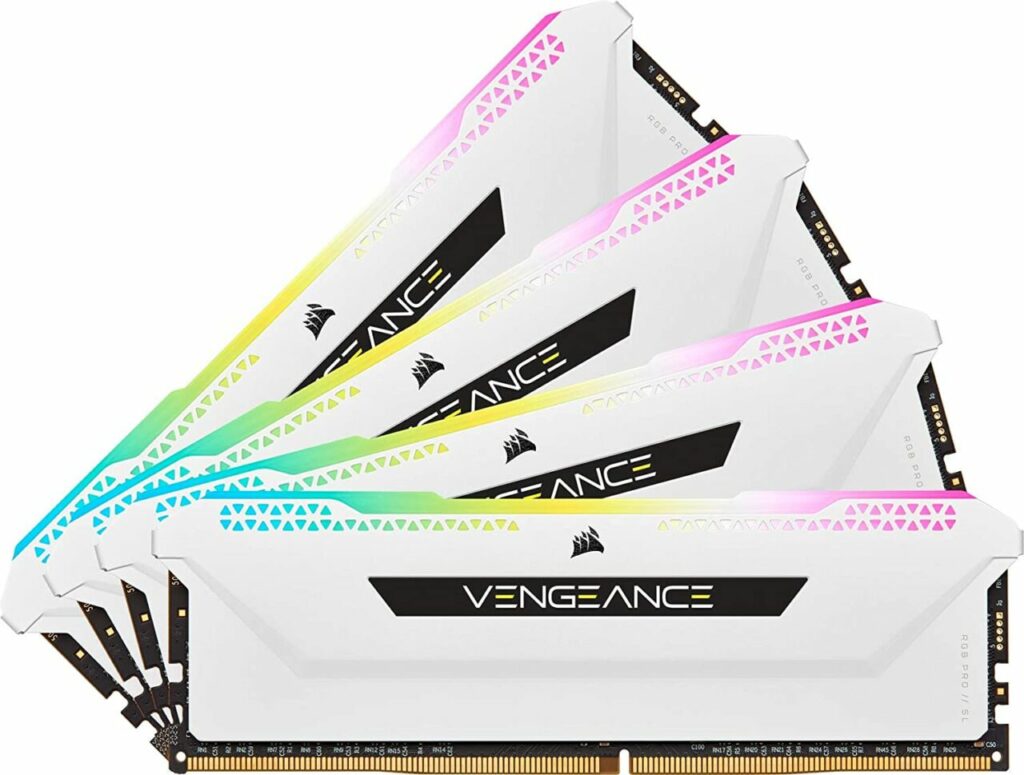
Dynamic random-access memory has its roots all the way to the first emergence of commercial computers in the 1970s. But DRAM as we are familiar with today (double-data-rate synchronous random-access memory), first became available with the development of Samsung‘s 64 MB memory chip in 1998.
Since then, DDR SDRAM became the technical standard for memory modules at the dawn of the 21st century. As its name suggests, DDR SDRAM mainly works by synchronizing data transfer and clock signals (frequency) at a double rate. That is, both the rise and fall, or “tick and tock” of each clock signal timing have a data value in it. This effectively doubles the data bus bandwidth without needing to increase the clock frequency. Each DDR version, as it is designated, featured various optimization tweaks, such as faster caching, more efficient power delivery, lower voltages, and higher clock frequencies. Most importantly, DDR SDRAM started the ball rolling on significantly increased bus bandwidth paired with much higher base data capacities.
DDR4 is the current DDR SDRAM standard in prevalent use for all modern PC builds today. It was first officially released last 2014, and features the highest efficiency and lowest data error (lowest need for data correction) in any DDR SDRAM modules ever produced. For perspective, first-generation DDR(1) sticks require a toasty 2.5 volts to operate normally, while DDR4 can nominally work using 1.2 volts (can be optimized further to 1.05 volts) thanks to significantly omitted data cycles removing additional (potentially useless) operations from the module. DDR4 is also the first DDR SDRAM to have no defined upper clock frequency limit. This is why you can see all the different high-end DDR4 memory modules with crazy frequencies that would have only been possible with overclocking before.
DDR5 brings even more optimization advancements to the table, significantly upping the ante on basic memory capacities. For example, it will finally have its power management module, rather than relying on motherboard memory VRMs for that function. Bandwidth is once again widened, from the baseline (non-custom, non-OC) 3.2Gbps of DDR4 to DDR5’s initial 4.8Gbps. Capacity per-die is no longer limited at 16GB, so the max 64GB of DDR4 will be 256GB for DDR5. In fact, according to Samsung, it can be pushed even higher.
Dynamic Flash Memory: When NAND Meets DRAM?
The specific research paper that introduced DFM, “Dynamic Flash Memory with Dual Gate Surrounding Gate Transistor (SGT)”, was showcased at the IEEE International Memory Workshop on May 18, 2021. The presenters were Koji Sakui, Nozomu Harada, with direct support from co-developer Fujio Masuoka.
How DRAM Normally Works
Traditional DRAM cells can store electrical charge in capacitors. The voltage spike from an electrical current provided by these components must be sufficient enough to be directly measurable, so that the flow can be addressed as a specific binary value. In effect, the capacitors become just as crucial as the accompanying transistors, making its reliance on constant power as a volatile data medium even more pronounced.
While operation remains relatively stable so long as power delivery is sustained, the stored charge eventually leaks, thus requiring constant recharge every now and then. Worse, when data is finally read into the memory, the charge is effectively drained, requiring the use of sense amplifiers to keep interpreting the binary values accurately.
This constant cycle of power delivery and outflow is described as inefficient, even as the technology itself got refined for the last couple of decades. The research then stresses the need for a proper replacement, that will prevent these power-hungry refresh cycles and destructive data reads from wasting a good chunk of the power and operational time given to the memory module.
What Dynamic Flash Memory Promises to Change
Enter Dynamic Flash Memory (DFM). According to Koji Sakui, DFM is set to more or less completely remove these design constraints by replacing the capacitor altogether with a pillar-like vertical structure as another standard FET (aptly named the FET SGT, or Field-effect Transistor/Surround Gate Transistor). So yeah, that means a cylindrical FET placed over a standard planar FET. Design technicalities aside, a vertical SGT with a fully realized, and production-level optimized design will change the memory game using several key factors:
- Better density per used area when compared to planar and sheet-stacked FinFET configurations
- Very little power leakage, thanks to the higher electrostatic control of the surrounding gate wrapped around the transistor channel
- An inherent (bonus) increase in data bandwidth. Since read/write delays due to power cycling becomes effectively non-existent, this means maximum bandwidth can be stretched somewhat considerably.
- Potential size reduction, or at least dimension alteration, for future DFM memory modules due to transistor shape and build.
Some people have pointed out the similarities that the stacked transistors have to store data cells in NAND Flash memory. For one thing, DFM transistors are not designed to be bit-erasable. This means that you have to rewrite the “memory cell” physically to reset binary values. This process also happens in block cycles (represented as a DFM array), making the resemblance all the more apparent. Pretty roundabout when compared to traditional DRAM. But hey, power costs way less, and response times are pretty fast, to say the least (20-30 ns).
Oh, but do take note that while capacitors are no longer needed to hold charge, this is still pretty much a volatile-type memory in operation. The DFM’s transistor would still inevitably leak power, just at a very significantly lower rate than a DRAM transistor. And if power is cut off, the values are reset as well.
Post-DRAM Tech World… Not Imminent?
Unisantis Electronics seems to be very proud of its announcement. In fact, the entire research team is ready to dismiss all other emerging memory module technologies unilaterally. They even declared (technically just hinted, albeit strongly) that their FET SGT memory transistor configuration will become the next memory module type moving forward.
Indeed, pretty bold statements, even for a founder of one of the most fundamentally used data technologies today (if he also represents the exact same opinion). But even in the face of such huge potential, DFM is going to hit a huge wall, represented by the entire development period and cost optimization that DRAM has experienced over the last couple of decades.
At the moment, we currently only have computer simulations to represent DFM as a technological concept. To compare, even when SATA already had physical working, commercial-level prototypes as early as 2002, it still took several years until it finally phased out the last IDE-based motherboards in 2008. With the team still several years away before any single prototype, any hope for something that would actually be plugged into our PCs is still a shot in the dark.
There is also the implementation. Due to the NAND Flash-like block-read/write cycles, its usage model will become markedly different from the traditional transistor+capacitor configuration for the equally power-feed dependent DRAM. Worst case scenario, the technology may require vastly different motherboard designs, offsetting its initial efficiency gains for the first decade of its mass implementation.
Final Thoughts
That being said, though, DFM has one industry-related ace up its sleeve right now: cost. Technological breakthroughs might be astonishing, but shattering the barrier of economics is arguably an even bigger achievement to strive for, if it is at all possible. And at least according to Unisantis’ calculations, DFM memory modules should be easier and cheaper to fabricate than conventional DRAMs. New production facilities and tools aside, each digital-bit would essentially use less material and be less physically complex.
This can potentially be a game-changer for the fluctuating memory module industry, an entity that is always at the whims of the entire electronic device production market. Perhaps in the far future, DFM memory module prices would be kept stabilized, and wouldn’t go up and down as much with the increase or decrease in demand for other devices that use memory modules, such as phones, tablets, or even modern cars.


