Intel Foveros: The Only Way is Up… Literally
32nm, 22nm, 16nm, 10nm. To the uninitiated, these seem like ordinary measurements, perhaps a standardized unit of some kind. But to the tech enthusiast, these figures represent the constant march of evolution in microchip technology. These measurements in a way, represent how we inch ever closer to the theoretical limit of Moore’s Law.
Intel, seeing the exponential challenges of manufacturing processors beyond 7nm, tried to look at a different approach in microchip architecture. Meet Foveros, the culmination of an initial solution to Intel’s production problems that, on paper, actually looks quite as simple as its initial proposal.

Promise of Invention: Intel’s 3D Initiative
The Embedded Multi-die Interconnect Bridge, or EMiB, is a technology that was implemented on Kaby Lake processors, first made available in 2018. It introduced a way to integrate thousands of interconnects between the processor’s GPU and memory.
How Foveros Adapts the Concept
This was achieved by a die configuration that traverses in three independently perpendicular directions, known as a face-to-face (F2F), chip-to-chip bonding. Whereas in 2D you can only create a few hundred interconnects side by side, when they’re stacked on top of one another in 3d, you can introduce interconnects on the whole face of the die, then wire each die along horizontally in an interposer layer.
This is the core concept that evolved later into Foveros. While EMiB previously used silicon “bridges” to create interconnects along an underlying package substrate (on separate dies), Foveros upgrades this to vertically combined dies connected via “microbumps”. Simply put, the stacking 3D connection was far more direct, essentially making the substrate layer itself its own microchip.
The application of this upgrade becomes important when we think about other components that can be stacked on such a configuration. For example, a hybrid microchip can stack DRAM dies together along with the base die, so that the connections simply go straight down, then the EMiB system is used to create the silicon “bridges” to connect at the other die placed laterally on the same layer.
Simple Concept, but Previously Never Strictly Necessary
From a retrospective angle, the idea actually seems kind of easy to conceive, laughably simple even. But we never had any technical reason to design such a processor until now. There usually was some sort of innovation or breakthrough that was a lot more economically feasible, such as multi-cores, better threading, optimized instruction sets, refined fabrication processes, among other innovations. Foveros, and even EMiB, was thus put back on the shelf several times over.
Today though, we are now struggling to get past 5nm, and consumer-grade CPUs are now reaching their general performance parameter limits due to most software still not fully optimized for parallel processing. With Foveros, Intel hopes to once again inspire innovation, and potentially open new frontiers for the industry.
Pressure Builds Up: Intel (and AMD) Loses Grip
But, why exactly was Intel pushed into developing Foveros now? Though development of newer chips has been typically portrayed as this epic struggle to keep up with Moore’s Law, the bigger factor has always been profits. Foveros may be a long-term investment, but it is still ultimately expected to supersede, or at least integrate, a lot of the technologies that keep Intel’s R&D well-funded.
So aside from just being a novel concept, Intel is also quite confident that Foveros will financially pay off due to the general state of CPUs today. As evidenced by these following two events, the industry is basically at a point in technology development where sustainability through more optimized products has become the more economic path.
Stringent Reaction to Intel’s Supply Shortage
Reinforcing the CPU market stalemate is Intel’s own direct blunder at failing to meet the demand for CPUs within the last few years. High-performing, reliable server units are absolutely vital to the likes of Amazon, Facebook, Tencent, and other big online service players. With Intel not delivering on time, their businesses can potentially be severely hampered.
In response, these companies have been trying to make their own chips in-house, using a licensing agreement with ARM instead, to remove their dependence on third-party component suppliers. And unlike Intel’s innovation-meets-profit strategy, they are quite happy to simply maintain profitability by optimizing ARM’s yesteryear tech. One example is Amazon’s Graviton CPU. Also, try counting the number of ARM-based laptops (that you would expect to be using an Intel CPU) that have been released for the last few years. The latest being the Microsoft Surface Pro X shown in the image below.

Microsoft Surface Pro X on Amazon
Sustainability Meets Innovation
With these companies seemingly trying to take AMD and Intel out of their economic equation, the pressure to keep profitability, or at least to mitigate recession losses, becomes even harder. While AMD frequently touts its “chiplet” technology as a performance boosting miracle, its implementation is actually more beneficial for the company’s production capability. AMD’s server-based EPYC CPUs for example, have the alternative option of being repurposed as Ryzen CPUs if the demand did not turn out to be what was expected, by simply reconfiguring the chiplets themselves.
All of these, combined with Intel’s think tank stagnation that occurred exactly during the time of AMD’s resurgence in the market, most likely helped accelerate the development of Foveros.
RELATED: ASUS ROG Zephyrus G14 Review: Powerful mobile gaming laptop and workstation
Foveros Forever: Lakefield Chips and Beyond
Just like its predecessor the EMiB, one important specification that Foveros is set to immediately provide huge improvements to is CPU memory bandwidth. While microchip companies have improved memory bandwidth through the years, the fact is CPU cache never really got out of the MB range, due to the inherent latency issues of dealing with a physically larger cache memory. Heck, we never even made it past two digits, as most consumer-grade (non-server) CPUs today still provide a technical maximum cache memory of 64 MB.
The ‘Complex’ Simplification
However, with the three-dimensional configuration of Foveros, hybrid processors using the technology can potentially bypass the physical limitations of using larger caches, allowing us to have significantly more without the drawbacks associated with it. We could easily zoom past the 3-digit limitation, with future more improved CPUs beyond Lakefield having probably as much as 1 GB of cache memory!
But a more practical application of the F2F 3D configuration of Foveros is just to simplify circuit design, to eliminate more parasitic elements on wiring lines. This in general will increase overall performance efficiency already, as it shortens the information relay “distance” between components. Additionally, this will also allow better parallelization of processed loads.
Not as Perfect, But it Works
Of course, the 3D stacking concept isn’t exactly as perfect as it seems. One direct consequence of stacking dies on top of one another is the build-up of heat. It was expected that Lakefield chips using Foveros tech would be offered at lowered clock speeds to provide an instant, albeit temporary, solution to this inherent issue.
Wouldn’t lowering clock speeds defeat the purpose of its performance improvements you ask? Intel has proven time and again, that optimizing chip configuration has been the better performance factor, not clock speed. For example, take a look at these two old processors from 2013-2014:
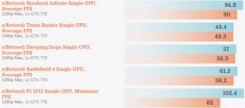
That is the FPS benchmark results for the Intel Core i5-4690K (teal), and AMD FX 9590 (orange). The FX 9590, despite having 5GHz clock speed, 4 cores and 8 threads, still managed to slightly lag behind the Corei5-4690K, which is configured at a significantly lower 3.7Ghz, 4 cores and 4 threads.
So even with a lowered clock speed due to perceived heating issues, we can still more or less expect Lakefield CPUs to be significantly more resource efficient than the competition (performance wise) during its first few iterations starting this year. At the very least, until AMD and ARM manages to compete with another breakthrough CPU architecture concept of their own.
Final Thoughts
As for us hapless enthusiasts watching from the sidelines, we can immediately expect Foveros to take mobile PC portability to new heights. Not too far unfortunately, but enough to once again squeeze more computing power per gram of hardware, and probably a few more hours of battery life. As for its price point, well, we can look at recently released Lakefield CPU-based products, such as the Samsung Galaxy Book S, to get a grasp on the package that you are supposed to expect.
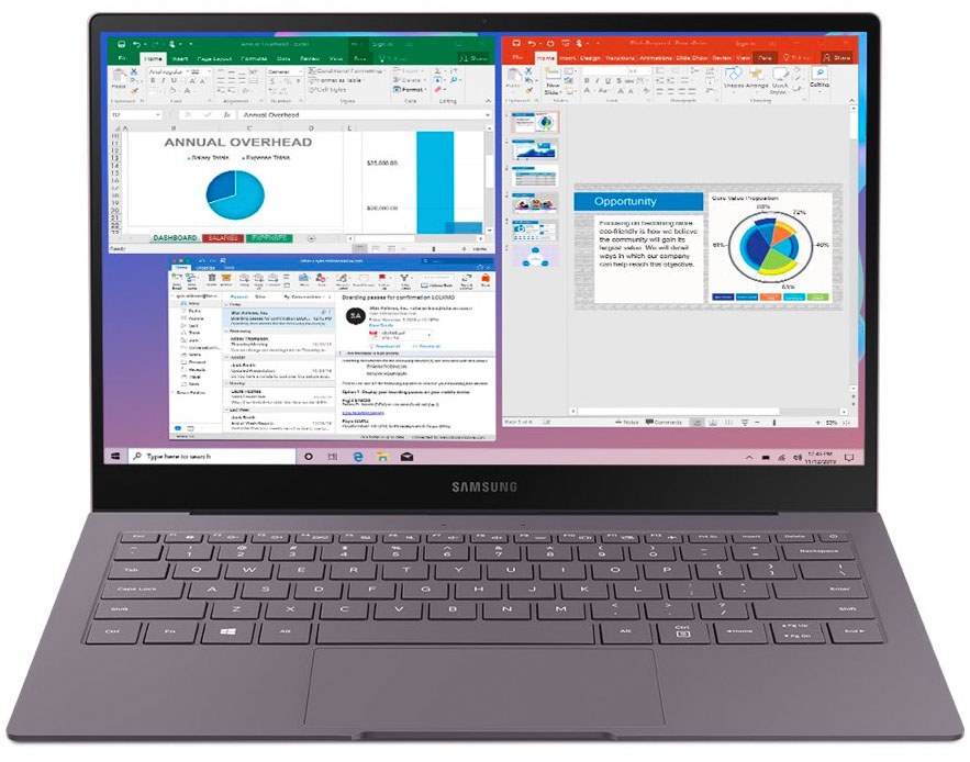
Samsung also launched the same laptop with competing ARM processor. Here is a quick look at the specifications comparing Intel’s Lakefield hybrid chip with Qualcomm Snapdragon 8cx ARM chip.
Comparing Samsung Galaxy Book S WiFi (Intel) vs Galaxy Book S LTE (Snapdragon)
| Galaxy Book S WiFi (Intel Lakefield) | Galaxy Book S LTE (Snapdragon) | |
|---|---|---|
| Operating System | Windows 10 Home | Windows 10 Home |
| Processor | Intel® Core™ i5-L16G7 | Qualcomm® Snapdragon™ 8cx Compute Platform Octa-core |
| Processor Speed | 1.4GHz | (4×2.84GHz + 4×1.8GHz) |
| Turbo Boost | 3.0GHz | n/a |
| Internal Memory 1, 2 | 8GB(RAM) + 256GB | 8GB(RAM) + 256GB |
| External Memory | MicroSD up to 2TB | MicroSD up to 1TB |
| Battery Capacity | 42 Wh | 42 Wh |
| Battery Run Time3 | Up to 17hrs video play time. | Up to 25 hours video play time. |
| Wireless PowerShare4 | No | No |
| Network Connectivity | Wi-Fi 6 (Gig+), 802.11 ax | LTE Cat.18 Nano SIM |
| Bluetooth | Bluetooth v5.0 | Bluetooth v5.0 |
| Other Connectivity | 2 USB-C | 2 USB-C |
| Colors | Mercury Gray, Earthy Gold | Mercury Gray |
| Screen Size | 13.3″ | 13.3″ |
| Resolution | 1920 x 1080 | 1920 x 1080 |
| Display Technology and Type | FHD LED | FHD LED |
| Touchscreen | Yes | Yes |
| Pen | No | No |
| Graphics | Intel® UHD Graphics | Shared |
| Sensors | Fingerprint Reader | Fingerprint Reader |
| Web Cam | 720p HD | 720p HD |
| Speakers | AKG Stereo Speakers | AKG Stereo Speakers |
| (1.2W x 4) | (1.2W x 4) | |
| Dolby Atmos | Dolby Atmos | |
| Audio Jack | 1 Headphone out/Mic-in Combo | 1 Headphone out/Mic-in Combo |
| Product Dimensions (L x W x H, inches) | 12.02 x 8.00 x 0.46″ | 12.02 x 8.00 x 0.46″ |
| Weight5 (pounds) | 2.09 lb | 2.12 lb |
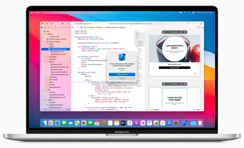
The competition is certainly heating up and the alternatives based on ARM chip as implemented here by Microsoft, Samsung and soon, Apple with their own Apple Silicon (also based on ARM chip) will push Intel to expand on their Lakefield offerings and beyond. The first commercially available system with Apple’s own System on Chip (SoC) will be available at the end of 2020. Developer’s already have access to Mac mini with Apple’s A12Z Bionic chip through Apple’s Developer Transition Kit (DTK).
In the next few decades though, with even better and more improved versions of the technology, a paradigm shift of the entire CPU design architecture philosophy will become even more likely to occur. Nothing on the scale of the first time multi-core CPUs were introduced though, but huge enough to make 3D stacking a considerable CPU design staple in the near future.


